单周期 CPU 数据通路设计 
约 1838 个字 337 行代码 2 张图片 预计阅读时间 10 分钟
Abstract
计算机系统 Ⅰ lab5-1 实验报告(2022.05.20 ~ 2022.06.10)
Warning
仅供学习参考,请勿抄袭
实验内容 
- 完成 32 位单周期 CPU 数据通路设计
- 实现 lw sw bne beq jal lui addi add slt slti 指令
- 根据提供的测试文件进行仿真测试
- 根据提供的测试环境进行上班验证
- bonus:指令扩展
- 实现 andi ori and or sll
- 实现 xori slli srli srl
- 实现 auipc sltu jalr
数据通路设计 
明确已给代码 
CPU 相关部分 
和单周期 CPU 本身有关的核心代码有
Control.v
通过 Control.edf 使用,在仿真时使用 Control_sim.v 文件中的 Control。功能是 CPU 的控制部分,其 Control 模块的输入输出部分:
input   [6:0]   op_code;
input   [2:0]   funct3;
input           funct7_5;
output  [1:0]   pc_src;
output          reg_write;
output          alu_src_b;
output  [3:0]   alu_op;
output  [1:0]   mem_to_reg;
output          mem_write;
output          branch;
output          b_type;
输出为译码得到的一些结果:
- pc_src:pc 来源,00 来自 pc+4、01 来自 JALR、10 来自 JAL
- reg_write:是否写入寄存器组
- alu_src_b:ALUsrc,0 表示 ALU 的第二个操作数来自寄存器,1 表示来自立即数
- alu_op:ALU 进行的操作符,在 AluOp.vh 中定义
- mem_to_reg:写回寄存器的数据来源,00 写回数据来自 ALU、01 来自立即数、10 来自 pc+4、11 来自 data memory
- mem_write:是否写入 data memory,0 表示读,1 表示写
- branch:指令是否是 branch 分支操作,1 表示是,0 不是
- b_type:分支操作类型,0 表示 bne、1 表示 beq
SCPU.v
单周期 CPU 结构文件,用于连接 CPU 的控制部分和数据通路部分,SCPU 模块输入输出部分:
input           clk,
input           rst,
input   [31:0]  inst,
input   [31:0]  data_in,  // data from data memory
input   [4:0]   debug_reg_addr,
output  [31:0]  addr_out, // data memory address
output  [31:0]  data_out, // data to data memory
output  [31:0]  pc_out,   // connect to instruction memory
output          mem_write,
output  [31:0]  debug_reg
输出有要操作 data memory 的地址 addr_out,要传给 data memory 的数据 data_out,接入 instruction memory 的 pc 指针值 pc_out,是否写入 data memory 的 mem_write,以及得到的 debug 要显示的寄存器值 debug_reg。
模块中间将 inst 拆分连接到了 Control 模块,再将 Control 模块的输出连接到 Datapath 的输入,Datapath 的输出作为 SCPU 的输出。
Core.v
将 SCPU 与 data memory(ip 核中的 RAM)和 instruction memory(ip 核中的 ROM)连接,并处理 SCPU 的时钟和 data memory 的时钟,再提供一些用于 debug 的输入输出
其它文件 
-
Top.sv
用于上板验证的顶层模块,其中将 Core 连接到了 IO_Manager 中来为 FPGA 板子提供输入输出的控制。
-
IO_Manager.sv
为 FPGA 板子提供输入输出的模块,其中处理了开发版上的按键、开关,以及七段管的输出。
-
Core_tb.sv
Core 模块的 test bench,进行仿真测试的时候将这个文件设为需要仿真的文件。
-
AluOp.vh
里面为 ALU 要进行的运算提供了变量名,实现 ALU 时要按照里面的规定来执行运算。
明确目标 
完成数据通路设计的目标有以下几个:
- 编写 ALU 模块,完成 AluOp.vh 文件中规定的运算
- 编写寄存器 Regs 模块,存储 31 个 32 位寄存器(第 0 个是 0
) ,处理寄存器的读写操作 - 编写一些 Mux 模块用于数据通路中的多路选择
- 编写 ImmGen 模块,用来从指令中解析出立即数
- 编写 Datapath 模块,连接起数据通路
- 在 SCPU 模块中正确连接 Control 与 Datapath(已经做好)
- 在 Core 模块中连接 SCPU 与 RAM ROM
模块编写与连接 
ALU
输入是两个 32 位数 a b 和进行的操作 alu_op,输出是结果和 zero 标志,case alu_op 然后分别实现就可以:
`timescale 1ns / 1ps

module ALU (
    input       [31:0]  a,
    input       [31:0]  b,
    input       [3:0]   alu_op,
    output reg  [31:0]  res,
    output              zero
);
    `include "AluOp.vh"
    always @(*) begin
        case (alu_op)
            ADD: res <= a + b;
            SUB: res <= a - b;
            SLL: res <= a << b;
            SLT: begin
                if (a[31] == 0 && b[31] == 1) res <= 0;
                else if (a[31] == 1 && b[31] == 0) res <= 1;
                else if (a[31] == b[31]) begin
                    if (a[30:0] < b[30:0]) res <= 1;
                    else res <= 0;
                end
            end
            SLTU: begin
                if (a < b) res <= 1;
                else res <= 0;
            end
            XOR: res <= a ^ b;
            SRL: res <= a >> b;
            SRA: res <= a >>> b;
            OR:  res <= a | b;
            AND: res <= a & b;
            default: res = 0;
        endcase
    end
    assign zero = (a-b) ? 1'b0 : 1'b1;
endmodule
寄存器 Regs 
在 lab 的 pdf 文件中已经给出了寄存器组部分的设计,只需要添加一下对于 debug_reg_addr 和 debug_reg 的输入输出即可:
`timescale 1ns / 1ps

module Regs (
    input           clk,
    input           rst,
    input           we,
    input   [4:0]   read_addr_1,
    input   [4:0]   read_addr_2,
    input   [4:0]   write_addr,
    input   [31:0]  write_data,
    input   [4:0]   debug_reg_addr,
    output  [31:0]  read_data_1,
    output  [31:0]  read_data_2,
    output  [31:0]  debug_reg
);
    integer i;
    reg [31:0] register [1:31]; // x1 - x31, x0 keeps zero

    assign read_data_1 = (read_addr_1 == 0) ? 0 : register[read_addr_1]; // read
    assign read_data_2 = (read_addr_2 == 0) ? 0 : register[read_addr_2]; // read
    assign debug_reg = (debug_reg_addr == 0) ? 0 : register[debug_reg_addr];

    always @(posedge clk or posedge rst) begin
        if (rst == 1) for (i = 1; i < 32; i = i + 1) register[i] <= 0; // reset
        else if (we == 1 && write_addr != 0) register[write_addr] <= write_data;
    end
endmodule
多路选择器 Mux 
首先实现普通的 32 位 2 路选择器 Mux2x32 和 32 位 4 路选择器 Mux4x32:
`timescale 1ns / 1ps

module Mux2x32 (
    input   [31:0]  I0,
    input   [31:0]  I1,
    input           s,
    output  [31:0]  o
);
    assign o = s ? I1 : I0;
endmodule

module Mux4x32 (
    input   [31:0]  I0,
    input   [31:0]  I1,
    input   [31:0]  I2,
    input   [31:0]  I3,
    input   [1:0]   s,
    output  [31:0]  o
);
    reg [31:0] out;
    always @(*) begin
        case (s)
            2'b00: out <= I0;
            2'b01: out <= I1;
            2'b10: out <= I2;
            2'b11: out <= I3;
        endcase
    end
    assign o = out;
endmodule
module MuxPC (
    input   [31:0]  I0,         // pc+4
    input   [31:0]  I1,         // JALR 的地址
    input   [31:0]  I2,         // JAL 的地址
    input   [31:0]  I3,         // branch 的地址
    input   [1:0]   s,          // pc_src
    input           branch,     // 是否分支
    input           b_type,     // 0 bne, 1 beq
    input   [31:0]  alu_res,    // alu 的结果,用来判断分支是否成立
    output  [31:0]  o           // 结果的 pc
);
    reg [31:0] out;
    always @(*) begin
        if (branch) begin // 有分支操作
            if (b_type) begin // beq
                if (alu_res == 32'b0)   out <= I3; // 分支
                else                    out <= I0;
            end
            else begin // bne
                if (alu_res == 32'b0)   out <= I0;
                else                    out <= I3; // 分支
            end
        end
        else begin
            case (s)
                2'b00: out <= I0;
                2'b01: out <= I1;
                2'b10: out <= I2;
                2'b11: out <= I3;
            endcase
        end
    end
    assign o = out;
endmodule
解析立即数 ImmGen 
先通过一个 Opcodes.vh 文件定义一些要用的指令名和 opcode 的对应以及指令类型的枚举:
//`ifndef OPCODES_H
//`define OPCODES_H
parameter   LW      = 7'b0000011,
            SW      = 7'b0100011,
            ADDI    = 7'b0010011,
            BNE     = 7'b1100011,
            BEQ     = 7'b1100011,
            JAL     = 7'b1101111,
            LUI     = 7'b0110111,
            ADD     = 7'b0110011,
            SLT     = 7'b0110011,
            SLTI    = 7'b0010011,
            ANDI    = 7'b0010011,
            ORI     = 7'b0010011,
            AND     = 7'b0110011,
            OR      = 7'b0110011,
            SLL     = 7'b0110011,
            XORI    = 7'b0010011,
            SLLI    = 7'b0010011,
            SRLI    = 7'b0010011,
            SRL     = 7'b0110011,
            AUIPC   = 7'b0010111,
            SLTU    = 7'b0110011,
            JALR    = 7'b1100111;

parameter   R   = 3'b000,
            I   = 3'b001,
            S   = 3'b010,
            B   = 3'b011,
            U   = 3'b100,
            J   = 3'b101;
//`endif
- R 型:20 个与 inst[31] 相同的符号位扩展比特和 inst[31:20]
- I 型:同 R 型
- S 型:20 个与 inst[31] 相同的符号位扩展比特和 inst[31:25] + inst[11:7]
- B 型:19 个与 inst[31] 相同的符号位扩展比特和 inst[31] + inst[7] + inst[30:25] + inst[11:8],最后一位补 0(相当于预先进行了分支时的 imm << 1 操作)
- U 型:inst[31:12] 后面补 12 个 0
- J 型:11 个与 inst[31] 相同的符号位扩展比特和 inst[31] + inst[19:12] + inst[20] + inst[30:21],最后一位补 0
根据这些规则以及指令和类型的对应可以写出 ImmGen 类:
`timescale 1ns / 1ps

module ImmGen(
    input   [31:0]  inst,
    output  [31:0]  imm
);
    `include "Opcodes.vh"
    reg [3:0] type;
    reg [31:0] out;
    assign imm = out;
    always @(*) begin
        case (inst[6:0])
            LW:     type <= I;
            SW:     type <= S;
            ADDI:   type <= I;
            BNE:    type <= B;
            BEQ:    type <= B;
            JAL:    type <= J;
            LUI:    type <= U;
            ADD:    type <= R;
            SLT:    type <= R;
            SLTI:   type <= I;
            ANDI:   type <= I;
            ORI:    type <= I;
            AND:    type <= R;
            OR:     type <= R;
            SLL:    type <= R;
            XORI:   type <= I;
            SLLI:   type <= R;
            SRLI:   type <= R;
            SRL:    type <= R;
            AUIPC:  type <= U;
            SLTU:   type <= R;
            JALR:   type <= I;
        endcase
        case (type)
            R: out <= {{20{inst[31]}}, inst[31:20]};
            I: out <= {{20{inst[31]}}, inst[31:20]};
            S: out <= {{20{inst[31]}}, inst[31:25], inst[11:7]};
            B: out <= {{19{inst[31]}}, inst[31], inst[7], inst[30:25], inst[11:8], 1'b0};
            U: out <= {inst[31:12], 12'b0};
            J: out <= {{11{inst[31]}}, inst[31], inst[19:12], inst[20], inst[30:21], 1'b0};
        endcase
    end
endmodule
数据通路 Datapath 
根据前面写好的模块以及分析,还有 pdf 给出的数据通路设计图就可以写出数据通路部分的代码:
`timescale 1ns / 1ps

module Datapath(
    input           clk,
    input           rst,
    input   [1:0]   pc_src,     // pc 来源
    input           reg_write,  // 是否写入寄存器
    input           alu_src_b,  // ALUsrc
    input           branch,     // 是否为 branch 类型的指令
    input           b_type,     // branch 类型
    input   [3:0]   alu_op,     // ALU operation
    input   [1:0]   mem_to_reg, // MemtoReg
    input   [31:0]  inst_in,    // 当前指令
    input   [31:0]  data_in,    // data from data memory
    output  [31:0]  addr_out,   // data memory address
    output  [31:0]  data_out,   // data to data memory
    output  [31:0]  pc_out,     // connect to instruction memory
    input   [4:0]   debug_reg_addr,
    output  [31:0]  debug_reg
);
    reg     [31:0]  pc;
    wire    [31:0]  pc_next;
    wire    [31:0]  write_data, read_data_1, read_data_2;
    wire    [31:0]  mux_out_1, alu_result;
    wire            alu_zero;
    wire    [31:0]  imm;
    wire    [31:0]  jmp_addr;

    assign pc_out = pc;
    assign addr_out = alu_result;
    assign data_out = read_data_2;

    always @(posedge clk or posedge rst) begin
        if (rst) begin
            pc <= 32'b0;        // 对 pc 复位
        end
        else begin
            pc <= pc_next;      // 设置 pc 的新值
        end
    end

    Regs regs (     // 连接寄存器组
        .clk(clk),
        .rst(rst),
        .we(reg_write),
        .read_addr_1(inst_in[19:15]),
        .read_addr_2(inst_in[24:20]),
        .write_addr(inst_in[11:7]),
        .write_data(write_data),
        .read_data_1(read_data_1),
        .read_data_2(read_data_2),
        .debug_reg_addr(debug_reg_addr),
        .debug_reg(debug_reg)
    );

    ImmGen immgen ( // 连接 ImmGen,从 inst_in 中获得立即数 imm
        .inst(inst_in),
        .imm(imm)
    );

    Mux2x32 mux2x32 (   // 选择 ALU 第二个输入
        .I0(read_data_2),
        .I1(imm),
        .s(alu_src_b),
        .o(mux_out_1)
    );

    ALU alu (   // 进行 ALU 运算,第一个输入是寄存器,第二个是选择器的结果
        .a(read_data_1),
        .b(mux_out_1),
        .alu_op(alu_op),
        .res(alu_result),
        .zero(alu_zero)
    );

    Mux4x32 mux4x32 (   // 选择写入 data memory 的数据
        .I0(alu_result),
        .I1(imm),
        .I2(pc + 4),
        .I3(data_in),
        .s(mem_to_reg),
        .o(write_data)
    );

    assign jmp_addr = pc + imm; // 得到跳转指令的跳转目标

    MuxPC mux_pc (  // 选择 pc 的新值
        .I0(pc + 4),    // 直接加 4
        .I1(jmp_addr),  // JALR 跳转地址
        .I2(jmp_addr),  // JAL 跳转地址
        .I3(jmp_addr),  // branch 跳转地址
        .s(pc_src),
        .branch(branch),
        .b_type(b_type),
        .alu_res(alu_result),
        .o(pc_next)     // pc 的新值
    );
endmodule
连接 RAM ROM 
直接将提供的 Ram.xci 和 Rom.xci 载入 vivado 就可以生成 ip 核,然后再 Core.v 文件中根据提示连接:
Rom rom_unit (
    .a(pc_out/4),   // 地址输入
    .spo(inst)      // 读数据输出
);

Ram ram_unit (
    .clka(mem_clk),         // 时钟
    .wea(mem_write),        // 是否写数据
    .addra(addr_out),       // 地址输入
    .dina(core_data_out),   // 写数据输入
    .douta(core_data_in)    // 读数据输出
);
Ram 的时钟要是 mem_clk 而不是 cpu_clk,不然会使 data memory 的输入输出被使用时错开一个周期,剩下的 mem_write、addr_out、core_data_out、core_data_in 都是 Core 模块中写好的从 SCPU 中获得的输出。
最后在 Core 末尾用于 debug 的部分根据提示来输出想要得到的寄存器的值:
这样整个数据通路的设计和整体的连接就完成了。
仿真测试 
vivado 中载入 ip 核的时候直接选择带有要求实现的全部十个指令 lw sw bne beq jal lui addi add slt slti 的 coe 参数文件 lab10_all.coe,与之对应的汇编文件就是 lab10_all.asm
然后选择 Core_tb.sv 为目标进行仿真测试,再通过调整得到全部中间变量(寄存器组值、ALU 输入输出、Mux 输入输出等)得到仿真波形:
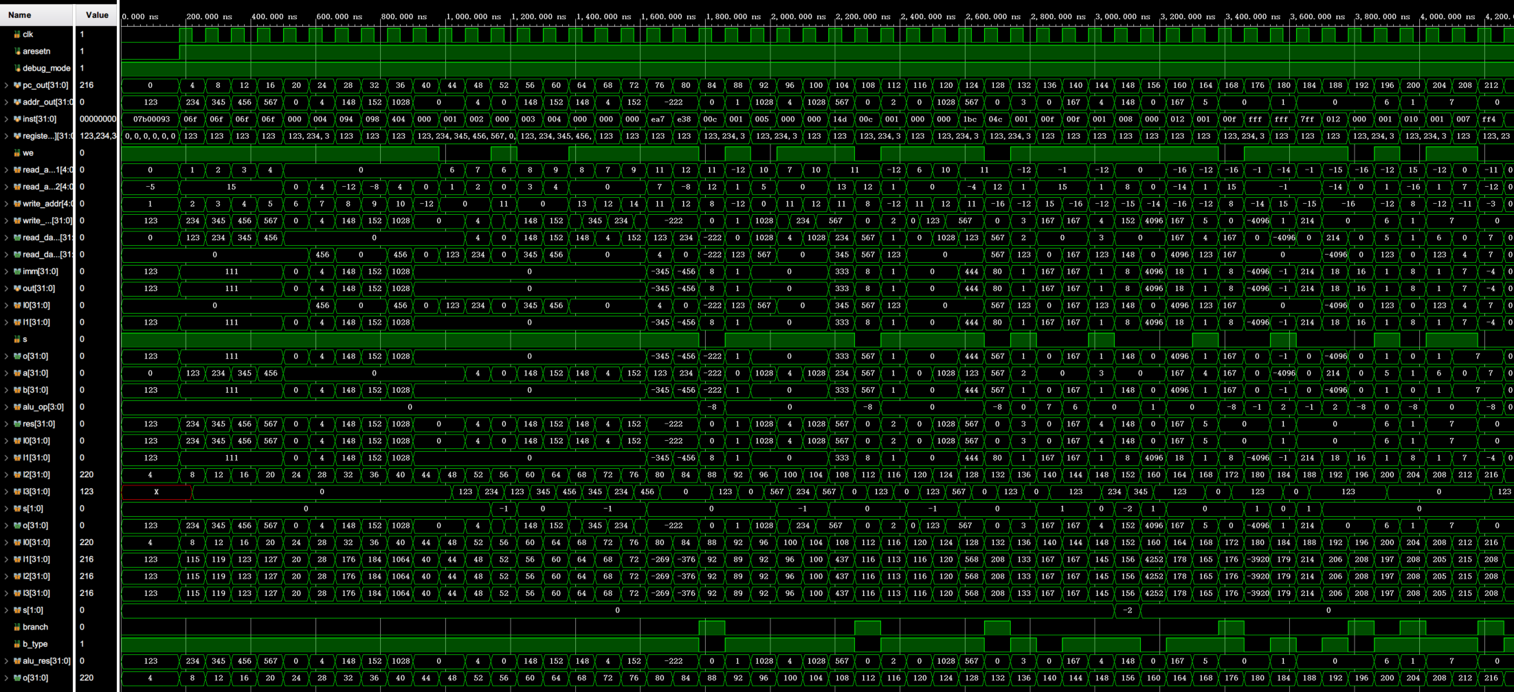
以及 pc 和寄存器的波形数据:

通过仔细分析每一条汇编指令与所有值的变化、寄存器的变化可以看出 CPU 按照给出的指令正确运行了。
上板验证 
在 vivado 中 disable 掉 Control_sim.v 文件(即使用 Control.v 和 Control.edf)然后通过 Top.sv 中顶层模块生成比特流,写入 FPGA 开发版即可进行上板验证。
通过单步运行,观察 pc、inst、寄存器值可以确定上板也没有任何问题。
Bonus
指令扩展部分放到下一个 lab 中跟随控制部分一起实现,写在下一次 lab 的实验报告中。